“This
is a milestone. It’s the first Processor that can use light to communicate with
the external world. No other Processor has the photonic I/O in the chip.”
Associate professor of
electrical engineering and computer sciences at the University of California,
Berkeley Vladimir Stojanovic, commenting on the development of a working Optical
Processor.
Optical
Processors may soon be possible within my lifetime.
A
collaboration between UC Berkeley and MIT (Massachusetts Institute of Technology)
has yielded a process that uses Optical pulses instead of electricity as
reported in the article “This
futuristic chip transmits data in an entirely new way”, published December
25, 2015 By Gabe Carey, Digitaltrends.
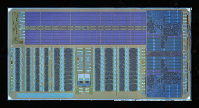 |
This
Processor, which consists of 70 million transistors and 850 photonic components
onto a 3-by-6-millimeter chip, isn't all Optical, as it still has to be powered
by electricity as noted in their publication in the Thursday December 24th
2015 print issue of the journal Nature!
The
main researchers on this project are all quite noteworthy:
1.
Mark Wade, Ph.D. student at the University
of Colorado, Boulder
2.
Yunsup Lee, a Ph.D. candidate at UC
Berkeley
3.
Jason Orcutt, an MIT graduate at IBM
Research Center in New York
In
their experiments, the researchers transmitted data to a receiver 10 meters in
a fiber optic loop as a test of its data transmission capabilities.
This
makes this Optical Processor more suited to be used in Switches and routers
rather than in Smartphone, tablets and computers to quote Associate professor
of electrical engineering and computer sciences at the University of
California, Berkeley Vladimir Stojanovic: “Light-based integrated circuits
could lead to radical changes in computing and network chip architecture in
applications ranging from smartphones to supercomputers to large data centers.
Something computer architects have already begun work on in anticipation of the
arrival of this technology”.
UC Berkeley and MIT Optical
Processor – Telecom Providers rejoice, consumer products coming
It’s
a huge breakthrough, as the data inputs into the Processor are all Optical and
its made in a foundry that mass-produces
high-performance computer chips as declared in the Press Release entitled “Engineers
demo first Processor that uses light for ultrafast communications”,
published DECEMBER 23, 2015 By Sarah Yang, Berkeley
News.
 |
They
fabricated the microprocessor in a foundry that mass-produces high-performance
computer chips, proving that their design can be easily and quickly scaled up
for commercial production.
This
is quite fortuitous and is similar to what I'd envisioned when IBM had
developed a Photonic Optical Processor as described in my blog article
entitled “IBM
develops 25Gbps Photonic Optical Processor at the 90nm level - IBM's Red Dawn
for Optical Processors”.
However
it may only find application initially in Router and Servers used in Telecom
Switches.
So
what does those this mean for Computer, Smartphone and Tablet Processors in the
Future?
UC Berkeley and MIT Optical
Processor – How the Optical Processor was made
Commercial production is around the corner, possibly
by 2020 as 5G is coming as reported in my blog article
entitled “ITU
publishes 5G IMT-2020 Roadmap - Why US Telecom Providers, @Digicel_Jamaica and
@LIMEJamaica like to travel off the beaten Path”.
The researchers deigned the Optical Processor to
communicate in light only. So no Optical to electrical conversion was done with
the chip. This means that the motherboard or chipset was fiber optic.
 |
The
researchers developed photonic I/O components to guide the UV light through the
Processor:
1.
Silicon waveguide
2.
Ring modulator
3.
Photodetector
4.
Vertical grating coupler
The
entire chip was fabricated using conventional process found in a typical
foundry that mass-produces high-performance computer chips. This makes
adjustments and optimization possible without any radical changes to the
fundamental process already being used to fabricate Processors.
First,
they made a few changes to the p and n type doping needed to make the
transistors as well as the etching masks so as to create the necessary Optical
waveguide traces within the silicon.
Once
that problem was cleared, they then had to develop an interface within the Processor
between the Optical input from the outside world, within the silicon waveguide
and the electrical parts of the Processor. They designed a Vertical grating
coupler that performed this task.
The
researchers took advantage of the fact that using the silicon doped with
germanium acts as a photodetector. Thus they used this unique property of
germanium to make a photodetector to read the UV Data pulses travelling along
the silicon Waveguide.
Transmission
was done via the use of the ring modulator which provided a low-energy
modulation of the UV light. This ring modulator had a p-n doped junction
connected to the silicon waveguide and effectively was a mini LED (Light
emitting Diode) that produced UV to send data along the waveguide to the
outside world.
Most
likely as the UV light leaves the Optical Processor via the vertical grating
coupler, an amplifier amplifies the light to be interpreted by the DSP (Digital
Signal Processor) as in a mobile device or Fiber optic modem as in a desktop
computer or router.
Ph.D.
candidate at CU-Boulder and a co-lead author of the study Mark Wade is
confident of this, quote: “We figured out how to reuse the same materials and
processing steps that comprise the electrical circuits to build
high-performance Optical devices in the same chip. This allows us to design
complex electronic-photonic systems that can solve the communication bottleneck
in computing”.
UC Berkeley and MIT Optical
Processor – Cool Operator that runs faster
This
Optical Processor demonstrates that faster Processors don't need to have more
power, as is the case with silicon Processors. The Optical Processor used 1.3
picojoules per bit, or roughly 1.3 watts of power for every terabit of data per
second!
|
By reducing the need to power a large motherboard
and a Processor as well as to convert data from Optical to electrics from the
DSP (Digital Signal Processor) in the case of a smartphone or the Fiber Optic
Modem in the case of a computer can make a computing device appear to be faster
at lower power levels.
This makes the Optical Processor suitable for
Routers and Switches for long haul Fiber Optic Networks as they’ll process data
without the need for Optical-electrical conversion as noted in “Chip
promises faster computing with light, not electrical wires”, published
December 23, 2015 by Stephen Shankland, CNET
News.
It also makes the device run cooler, making it
possible to reach faster speeds without having to increase cooling
requirements.
UC
Berkeley and MIT Optical Processor - Optical Bandwidth just in time for 5G in
2020
This Optical Processor has benefits in terms of
bandwidth, as the data input and output is Optical, allowing the dual-core
design to process more data.
According to the researchers, it can process some 300
gigabits per second per square millimeter, about 10 to 50 times greater than
its electronic counterparts!
The fact that it directly processes Optical Data
means that the Developement of Li-Fi Networks can progress unhindered by
limitations of the Devices as noted in my blog article
entitled “Why
pureLiFi Solar Powered Li-Fi is coming to Apple iPhone with 5G Internet by 2020”.
This development will be bang on time as 5G is
expected in 2020. Expect similar tech to be licensed and used in smartphones,
Tablets, Smart TV as well as desktop computers by 2020.
No comments:
Post a Comment